Monday, July 20, 2020

Running Simple DirectX12 Compute Shader: Looking into Dispatch xyz, numthreads xyz, SV_GroupIndex and SV_GroupID xyz

There are many arguments to run compute shader and many arguments are passed to compute shader main function.

On this post, a computer shader is executed with
  • Dispatch(4,1,1)
  • numthreads(3,1,1)
to see what argument values are passed to compute shader main function.

Source code

Compute shader: https://sourceforge.net/p/playpcmwin/code/HEAD/tree/PlayPcmWin/WWDirectCompute12Test2019/Sandbox.hlsl

C++ program to run the compute shader: https://sourceforge.net/p/playpcmwin/code/HEAD/tree/PlayPcmWin/WWDirectCompute12Test2019/TestSandboxShader.cpp

Compute shader to run on the GPU

Sandbox.hlsl : this compute shader is called with Dispatch(4,1,1)
RWStructuredBuffer<float> g_output   : register(u0);

[numthreads(3, 1, 1)]
void
CSMain(
    uint tid : SV_GroupIndex,                 // 0 <= tid < 3 ← numthreads(3,1,1)
    uint3 groupIdXYZ : SV_GroupID)   // 0 <= groupIdXYZ.x < 4
Dispatch(xyz=(4,1,1))
{
    int idx = tid + groupIdXYZ.x * 5;
    g_output[idx] = 1;
}

Shader setup

Please refer TestSandboxShader.cpp. It compiles Sandbox.hlsl as a compute shader, prepares GPU buffer of 4096 bytes and sets Unordered Access View, creates compute state, calls Dispatch(4,1,1), and copy GPU buffer memory values to CPU memory of float array.
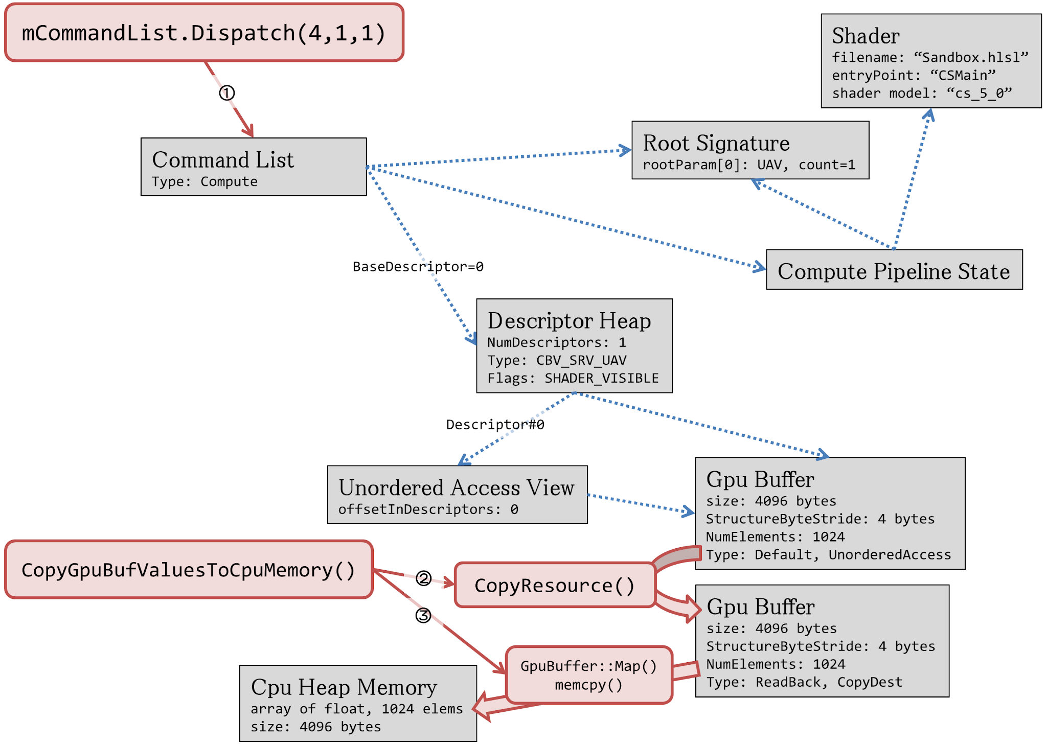

Compute Shader resources, shader main function arguments and thread group

Unordered Access View u0 is visible from the compute shader. Shader can read/write to this buffer.

CSMain function is called 12 times total, function argument of each call is as follows:
CSMain(tid=0, groupIdXYZ=0,0,0)
CSMain(tid=1, groupIdXYZ=0,0,0)
CSMain(tid=2, groupIdXYZ=0,0,0)

CSMain(tid=0, groupIdXYZ=1,0,0)
CSMain(tid=1, groupIdXYZ=1,0,0)
CSMain(tid=2, groupIdXYZ=1,0,0)

CSMain(tid=0, groupIdXYZ=2,0,0)
CSMain(tid=1, groupIdXYZ=2,0,0)
CSMain(tid=2, groupIdXYZ=2,0,0)

CSMain(tid=0, groupIdXYZ=3,0,0)
CSMain(tid=1, groupIdXYZ=3,0,0)
CSMain(tid=2, groupIdXYZ=3,0,0)
3 subsequent calls share the same groupIdXYZ and those 3 calls are executed "simultaneously": GPU has several hundred cores. 3 tasks are assigned to 3 individual GPU cores and they runs in parallel (See the following image). On more practical compute shader, it is important to run 128 or more shaders in parallel: something like numthreads(128,1,1) to utilize GPU cores fully.
Those 3 function calls that shares the same groupIdXYZ is called the thread group. GPU function calls of the same thread group can share thread group shared memory (TGSM) that is significantly faster than UAV memory, while TGSM size is limited to 32 KB or so. Utilizing TGSM is one of the key technique to accelerate GPU computation.

On this Sandbox compute shader, each shader writes adjacent GPU memory position simultaneously. This slows down write operation. It is better for each threadgroup threads to write to more remote memory position each other to write data more quickly.

Values written to u0 GPU memory

Sandbox.hlsl shader writes those values to the GPU buffer memory u0:g_Output.
    i, g_output[i], Shader function args to write this value
    0, 1.000000,   <== CSMain(tid=0, groupIdXYZ=0,0,0)
    1, 1.000000,   <== CSMain(tid=1, groupIdXYZ=0,0,0)
    2, 1.000000,   <== CSMain(tid=2, groupIdXYZ=0,0,0)
    3, 0.000000,
    4, 0.000000,
    5, 1.000000,   <== CSMain(tid=0, groupIdXYZ=1,0,0)
    6, 1.000000,   <== CSMain(tid=1, groupIdXYZ=1,0,0)
    7, 1.000000,   <== CSMain(tid=2, groupIdXYZ=1,0,0)
    8, 0.000000,
    9, 0.000000,
   10, 1.000000,   <== CSMain(tid=0, groupIdXYZ=2,0,0)
   11, 1.000000,   <== CSMain(tid=1, groupIdXYZ=2,0,0)
   12, 1.000000,   <== CSMain(tid=2, groupIdXYZ=2,0,0)
   13, 0.000000,
   14, 0.000000,
   15, 1.000000,   <== CSMain(tid=0, groupIdXYZ=3,0,0)
   16, 1.000000,   <== CSMain(tid=1, groupIdXYZ=3,0,0)
   17, 1.000000,   <== CSMain(tid=2, groupIdXYZ=3,0,0)
   18, 0.000000,
   19, 0.000000,
   20, 0.000000,
   21, 0.000000,
   22, 0.000000,
   23, 0.000000,
   24, 0.000000,


Saturday, July 11, 2020

Benchmark: maxCache accelerated HDD RAID10 array

I tried to to accelerate a HDD raid array by connecting a SAS12G SSD to Adaptec raid controller as a maxCache 4.0 device.

Connecting the SSD to Controller

Set the connector to HBA mode on maxView.
On Linux, type dmesg to find drive device file name:

 # dmesg
           ...
[  817.729986] smartpqi 0000:41:00.0: added 10:0:-:- 5000c5003e8f4f3d Direct-Access     SEAGATE  XS960SE70004     AIO+ qd=64

[  817.732450] scsi 10:0:1:0: Direct-Access     SEAGATE  XS960SE70004     0004 PQ: 0 ANSI: 7
[  817.733837] sd 10:0:1:0: Attached scsi generic sg5 type 0
[  817.736622] sd 10:0:1:0: [sdd] 1875385008 512-byte logical blocks: (960 GB/894 GiB)
[  817.736625] sd 10:0:1:0: [sdd] 4096-byte physical blocks
[  817.737389] sd 10:0:1:0: [sdd] Write Protect is off
[  817.737391] sd 10:0:1:0: [sdd] Mode Sense: dd 00 10 08
[  817.738855] sd 10:0:1:0: [sdd] Write cache: disabled, read cache: enabled, supports DPO and FUA
[  817.754703] sd 10:0:1:0: [sdd] Attached SCSI disk

It seems my drive is /dev/sdd and /dev/sg5. And drive logical sector size is 512: It is ready to use it as a maxCache drive. Set the connector to RAID mode on maxView.

Using it as a maxCache drive

Enable maxCache to HDDx8 Raid10 array, it is something similar steps as a last article.

Test setup  

  • AMD ThreadRipper 2990WX
  • Memory 64GB
  • Microsemi Adaptec SmartRaid 3154-8i16e (memory cache is enabled)
  • HDD: WDC WD40EZRZ-00G 3.5inch SATA HDD x8 RAID10
  • SSD for MaxCache: Seagate Nytro XS960SE70004 SAS12G SSD
  • Windows 10 x64 version 2004

Benchmark results

CrystalDiskMark 7.0.0

Fig. 1 HDDx8 RAID10 without maxCache


Fig.2 HDDx8 RAID10 with maxCache of 1 SSD (unsafe)


Fig.3 HDDx8 RAID10 with maxCache of 2 SSD RAID1

Some thoughts about the result


It seems maxCache4.0 works well. Especially read performance is accelerated. HDD array performs like a SSD.

Write performance is better than ordinal HDD even without maxCache. I suppose this is thanks to the 4GB memory cache of the raid controller.

Disabling maxCache

On maxView, wait until super capacitor is charged. Select raid array and press Set Properties button of Logical Device ribbon group. move to maxCache tab and select  Set Write cache policy preferred to Write Through. Wait until SSD cache data is flushed to HDD. then select maxCacheDevice → deviceName → Cache for ArrayName, Press the Delete maxCache button on maxCache ribbon group.

Disk Provisioning

Seagate Nytro 3331 SSD accepts provision command on SeaChest_Basics utility. I reduced drive capacity from 960GB to 800GB (1562500000 LBA) to increase drive write endurance (I hope).

Set controller connector connected to Nytro SSD to HBA mode. Then run following command on the Linux console:
# cd SeaChest/Linux/Lin64/
# ./SeaChest_Basics_280_11923_64 --scan --onlySeagate

to find your seagate SSD. In my case it is /dev/sg1

# ./SeaChest_Basics_280_11923_64 -d /dev/sg1 -i

to see MaxLBA size. My drive MaxLBA is 1875385007 (approx. 960GB). 

Reduce drive capacity to 800GB (LBA 156250000 ): 


# ./SeaChest_Basics_280_11923_64 -d /dev/sg1 --provision 1562500000 

Then reboot the computer.

Set controller connector connected to Nytro SSD to RAID mode to use it as a maxCache drive.

Current Storage Configuration


Following maxView screen shows current configuration of my storage array.


Sunday, June 7, 2020

Setting up maxCache device using Intel SSD DC S4500

Microsemi Adaptec SmartRaid 3154-8i16e has a maxCache 4.0 feature, to accelerate HDD IO using SSD as a cache.

SSD with 512 bytes sector is required for maxCache drive.

I purchased 2 Intel SSD DC S4500 240GB SATA drives (Please read the last part of this article about suitability of this drive to this usage) to create RAID1 maxCache array. Those SSDs' physical block size is 4KB by default (Fig.1), but it can be changed to 512 bytes using Intel Memory and Storage tool.

Fig.1 Physical block size of this SSD is 4KB by default.

How to set 512 bytes sector size to Intel SSD DC S4500


1. Connect SSDs to Adaptec and expose it as RAW device to the operating system.


Connect 2 SSDs to Adaptec. Open maxView. Select controller and press Controller Set Properties on Connector tab, set the connector connected to Intel SSDs to HBA mode (Fig.3). This exposes raw SSD devices to the OS and Intel MAS is able to work with them. The two devices shows up as a /dev/sdd and /dev/sde respectively.


Fig.2 : Two intel SSDs are connected to Connector #1. Connector mode is changed to HBA mode.

BTW I performed burn-in to one of the two SSDs using shred -n=10 -z command and 1 day powered idle to prevent simultaneous two drive failure.


2. Set sector size to 512B using Intel Memory and Storage Tool 


Download and install Intel Memory and Storage tool (CUI) for your operating system.

Run intelmas to show device index. In my computer, two Intel SSDs have index #3 and #4.
# intelmas show -intelssd

To set 512 bytes sector size to device #3,
# intelmas set -intelssd 3 PhysicalSectorSize=512

Disconnect SSD and reconnect to reflect the change.

Repeat it to the second SSD.

if your SSD firmware is old, it can be updated with the following command (disconnect SSD and reconnect to boot SSD with updated firmware):
# intelmas load -intelssd 3

Set Connector connected to Intel SSDs to RAID mode on MaxView Storage Manager. Now those 2 drives' physical sector size is 512 bytes and ready to create maxCache array (Fig.3)


Fig.3 : Physical block size is now 512 bytes.

Now those drives can be used as maxCache drives.

Creating maxCache array of 2 SSD RAID1


Open maxView. Select Controller and press Create maxCache device button (Fig.4)


Fig.4 : Create maxCache device button is far right of the menu bar.

On Create maxCache device menu, select RAID 1, press next (Fig.5).


Fig.5

Select 2 Intel SSDs to raid member drives. press next (Fig.6).

Fig.6

Select HDD drive array to accelerate performance. press next (Fig.7).

Fig.7 : Select HDD array to accelerate.

Set RAID attribute. leave as default. press next (Fig.8).

Fig.8

Summary is shown. press Finish (Fig.9).


Fig.9

Now maxCache array is created and started to work (Fig.10) (Fig.11).


Fig.10


Fig.11
It seems maxCache works.


SSD write performance is important for maxCache drive!


Use it a while and found HDD IO performance is not so accelerated as I expected. And found my SSDs' effective write speed is surprisingly low, about 130MB/sec and it is about the same level of single HDD drive! Max sequential write of this drive is 190MB according to the datasheet: https://ark.intel.com/content/www/us/en/ark/products/120526/intel-ssd-dc-s4500-series-240gb-2-5in-sata-6gb-s-3d1-tlc.html

Also noticed the controller writes extensively to maxCache drives, so moderately high PBW value is necessary. In my use case and HDD array capacity, order of 0.1 ~ 1.0 PBW is needed.

Therefore high IO performance and some level of PBW value (this differs depending on the use case and array capacity) are important to the drive used as maxCache device. And I'm now looking into the datasheets of SAS SSDs ...


Next Article, benchmarking with proper SAS12G SSD: https://yamamoto2002.blogspot.com/2020/07/benchmarking-maxcache-40-with-sas12g-ssd.html

Wednesday, April 29, 2020

Microsemi Adaptec SmartRAID 3154-8i16e connector numberings

I'm a fan of Adaptec storage adapters since AHA-1542B 😄

Today I looked into connector numbering of SmartRAID 3154-8i16e, awesome hardware RAID controller card. It seems there is no info regarding to this topic on the net!

This card has 4 external HD mini-SAS connectors and 2 internal HD mini-SAS connectors. When SAS expander or port multiplier is not used, each HD mini-SAS connectors accommodate 4 SATA or SAS drives. Therefore up to 24 SAS or SATA drives can be connected directly to this card.

Fig.1 SmartRAID 3154-8i16e connector numberings

Connector Numbering Scheme

There is a Connector id and CN id, these are differently numbered. From the observation, numbering scheme is as follows:
  • Connector number starts with internal HD mini-SAS connector to mate to SFF-8643 and external HD mini-SAS to mate to SFF-8644.
  • CN number starts with external HD mini-SAS and continue with internal HD mini-SAS.
  • Both numbers are assigned from the connector of the bottom of the card to the top.


About Slot Number


Slot number is assigned to these SAS/SATA ends. From the observation, slot number starts from 1, Connector 0 (CN4) has Slot 1, 2, 3 and 4. Connector 1 (CN5) has Slot 5, 6, 7 and 8, and things goes on.

Connector 0 CN4 Internal HD mini-SAS Slot 1,2,3,4
Connector 1 CN5 Internal HD mini-SAS Slot 5,6,7,8
Connector 2 CN0 External HD mini-SAS Slot 9,10,11,12
Connector 3 CN1 External HD mini-SAS Slot 13,14,15,16
Connector 4 CN2 External HD mini-SAS Slot 17,18,19,20
Connector 5 CN3 External HD mini-SAS Slot 21,22,23,24

SFF-8643 to 4 SATA fan-out cable connector numbering


This is a picture of my Microsemi Adaptec HD mini-SAS to 4 SATA fan-out cable, part # 2279800-R. Number tags are attached on each SATA connectors and this number starts from 0.

Fig.2 Closeup photo of SATA connectors of SFF-8643 to 4 SATA fan-out cable 2279800-R.


MaxView Storage Manager Physical Devices View


MSM shows physical drive placement as follows:

(In the following example, drives are populated only on the external connectors. Following image is pictured during a test of automatic rebuild therefore RAID array is rebuilding.)

Fig.3 MaxView Physical device list


Saturday, September 28, 2019

Benchmark: Cross-NUMA remote memory access cost and real world app

Cross-NUMA remote memory access cost of Intel Xeon E5-2650v3 2CPU computer is investigated.


Coreinfo


Cross-NUMA memory access cost is calculated using SysInternals coreinfo


C:\apps\SysinternalsSuite>coreinfo

Coreinfo v2.11 - Dump information on system CPU and memory topology
Copyright (C) 2008-2010 Mark Russinovich
Sysinternals - www.sysinternals.com

(snip)

Approximate Cross-NUMA Node Access Cost (relative to fastest):
       00  01
00: 1.0 1.3
01: 1.4 1.1

According to coreinfo, cross-NUMA access cost is 1.3 to 1.4 (remote memory is 30 to 40 % slower than local memory)

WWAudioFilter 1.0.54


Test setup: add jitter with convolution length=65537 to 1800 second 44100Hz mono WAV file.


Result

  • Allocate memory on NUMA0, process on NUMA0 CPU: 52 min 29.6 sec
  • Allocate memory on NUMA0, process on NUMA1 CPU: 52 min 31.2 sec
  • Using all resources: 26 min 52.5 sec

Thoughts


  • On this NUMA computer, Using coreinfo, remote memory access is 30 to 40 percent slower than local memory access.
  • WWAudioFilter 1.0.54 does not show cross-NUMA performance degradation. Perhaps it is because all input data to processing is cached on CPU and core does not stall (wait until data is arrived). Also the problem is double precision math and it takes time to compute so it is compute intensive and this is not memory bottle-necked workload.


 computing on NUMA0 core, processing load graph per NUMA node.

 computing on NUMA0 core, processing load graph per logical core.

computing on NUMA1 core, processing load graph per NUMA node.


Appendix A. Full coreinfo result

This computer has 2 CPUs, each CPU has 10 core. Windows accommodates all the core to single processor group so it is very easy to scale for any apps. Last level CPU cache size is 25MB.

C:\apps\SysinternalsSuite>coreinfo

Coreinfo v2.11 - Dump information on system CPU and memory topology
Copyright (C) 2008-2010 Mark Russinovich
Sysinternals - www.sysinternals.com

Logical to Physical Processor Map:
**-------------------------------------- Physical Processor 0 (Hyperthreaded)
--**------------------------------------ Physical Processor 1 (Hyperthreaded)
----**---------------------------------- Physical Processor 2 (Hyperthreaded)
------**-------------------------------- Physical Processor 3 (Hyperthreaded)
--------**------------------------------ Physical Processor 4 (Hyperthreaded)
----------**---------------------------- Physical Processor 5 (Hyperthreaded)
------------**-------------------------- Physical Processor 6 (Hyperthreaded)
--------------**------------------------ Physical Processor 7 (Hyperthreaded)
----------------**---------------------- Physical Processor 8 (Hyperthreaded)
------------------**-------------------- Physical Processor 9 (Hyperthreaded)
--------------------**------------------ Physical Processor 10 (Hyperthreaded)
----------------------**---------------- Physical Processor 11 (Hyperthreaded)
------------------------**-------------- Physical Processor 12 (Hyperthreaded)
--------------------------**------------ Physical Processor 13 (Hyperthreaded)
----------------------------**---------- Physical Processor 14 (Hyperthreaded)
------------------------------**-------- Physical Processor 15 (Hyperthreaded)
--------------------------------**------ Physical Processor 16 (Hyperthreaded)
----------------------------------**---- Physical Processor 17 (Hyperthreaded)
------------------------------------**-- Physical Processor 18 (Hyperthreaded)
--------------------------------------** Physical Processor 19 (Hyperthreaded)

Logical Processor to Socket Map:
********************-------------------- Socket 0
--------------------******************** Socket 1

Logical Processor to NUMA Node Map:
********************-------------------- NUMA Node 0
--------------------******************** NUMA Node 1

Approximate Cross-NUMA Node Access Cost (relative to fastest):
00 01
00: 1.0 1.3
01: 1.4 1.1

Logical Processor to Cache Map:
**-------------------------------------- Data Cache 0, Level 1, 32 KB, Assoc 8, LineSize 64
**-------------------------------------- Instruction Cache 0, Level 1, 32 KB, Assoc 8, LineSize 64
**-------------------------------------- Unified Cache 0, Level 2, 256 KB, Assoc 8, LineSize 64
********************-------------------- Unified Cache 1, Level 3, 25 MB, Assoc 20, LineSize 64
--**------------------------------------ Data Cache 1, Level 1, 32 KB, Assoc 8, LineSize 64
--**------------------------------------ Instruction Cache 1, Level 1, 32 KB, Assoc 8, LineSize 64
--**------------------------------------ Unified Cache 2, Level 2, 256 KB, Assoc 8, LineSize 64
----**---------------------------------- Data Cache 2, Level 1, 32 KB, Assoc 8, LineSize 64
----**---------------------------------- Instruction Cache 2, Level 1, 32 KB, Assoc 8, LineSize 64
----**---------------------------------- Unified Cache 3, Level 2, 256 KB, Assoc 8, LineSize 64
------**-------------------------------- Data Cache 3, Level 1, 32 KB, Assoc 8, LineSize 64
------**-------------------------------- Instruction Cache 3, Level 1, 32 KB, Assoc 8, LineSize 64
------**-------------------------------- Unified Cache 4, Level 2, 256 KB, Assoc 8, LineSize 64
--------**------------------------------ Data Cache 4, Level 1, 32 KB, Assoc 8, LineSize 64
--------**------------------------------ Instruction Cache 4, Level 1, 32 KB, Assoc 8, LineSize 64
--------**------------------------------ Unified Cache 5, Level 2, 256 KB, Assoc 8, LineSize 64
----------**---------------------------- Data Cache 5, Level 1, 32 KB, Assoc 8, LineSize 64
----------**---------------------------- Instruction Cache 5, Level 1, 32 KB, Assoc 8, LineSize 64
----------**---------------------------- Unified Cache 6, Level 2, 256 KB, Assoc 8, LineSize 64
------------**-------------------------- Data Cache 6, Level 1, 32 KB, Assoc 8, LineSize 64
------------**-------------------------- Instruction Cache 6, Level 1, 32 KB, Assoc 8, LineSize 64
------------**-------------------------- Unified Cache 7, Level 2, 256 KB, Assoc 8, LineSize 64
--------------**------------------------ Data Cache 7, Level 1, 32 KB, Assoc 8, LineSize 64
--------------**------------------------ Instruction Cache 7, Level 1, 32 KB, Assoc 8, LineSize 64
--------------**------------------------ Unified Cache 8, Level 2, 256 KB, Assoc 8, LineSize 64
----------------**---------------------- Data Cache 8, Level 1, 32 KB, Assoc 8, LineSize 64
----------------**---------------------- Instruction Cache 8, Level 1, 32 KB, Assoc 8, LineSize 64
----------------**---------------------- Unified Cache 9, Level 2, 256 KB, Assoc 8, LineSize 64
------------------**-------------------- Data Cache 9, Level 1, 32 KB, Assoc 8, LineSize 64
------------------**-------------------- Instruction Cache 9, Level 1, 32 KB, Assoc 8, LineSize 64
------------------**-------------------- Unified Cache 10, Level 2, 256 KB, Assoc 8, LineSize 64
--------------------**------------------ Data Cache 10, Level 1, 32 KB, Assoc 8, LineSize 64
--------------------**------------------ Instruction Cache 10, Level 1, 32 KB, Assoc 8, LineSize 64
--------------------**------------------ Unified Cache 11, Level 2, 256 KB, Assoc 8, LineSize 64
--------------------******************** Unified Cache 12, Level 3, 25 MB, Assoc 20, LineSize 64
----------------------**---------------- Data Cache 11, Level 1, 32 KB, Assoc 8, LineSize 64
----------------------**---------------- Instruction Cache 11, Level 1, 32 KB, Assoc 8, LineSize 64
----------------------**---------------- Unified Cache 13, Level 2, 256 KB, Assoc 8, LineSize 64
------------------------**-------------- Data Cache 12, Level 1, 32 KB, Assoc 8, LineSize 64
------------------------**-------------- Instruction Cache 12, Level 1, 32 KB, Assoc 8, LineSize 64
------------------------**-------------- Unified Cache 14, Level 2, 256 KB, Assoc 8, LineSize 64
--------------------------**------------ Data Cache 13, Level 1, 32 KB, Assoc 8, LineSize 64
--------------------------**------------ Instruction Cache 13, Level 1, 32 KB, Assoc 8, LineSize 64
--------------------------**------------ Unified Cache 15, Level 2, 256 KB, Assoc 8, LineSize 64
----------------------------**---------- Data Cache 14, Level 1, 32 KB, Assoc 8, LineSize 64
----------------------------**---------- Instruction Cache 14, Level 1, 32 KB, Assoc 8, LineSize 64
----------------------------**---------- Unified Cache 16, Level 2, 256 KB, Assoc 8, LineSize 64
------------------------------**-------- Data Cache 15, Level 1, 32 KB, Assoc 8, LineSize 64
------------------------------**-------- Instruction Cache 15, Level 1, 32 KB, Assoc 8, LineSize 64
------------------------------**-------- Unified Cache 17, Level 2, 256 KB, Assoc 8, LineSize 64
--------------------------------**------ Data Cache 16, Level 1, 32 KB, Assoc 8, LineSize 64
--------------------------------**------ Instruction Cache 16, Level 1, 32 KB, Assoc 8, LineSize 64
--------------------------------**------ Unified Cache 18, Level 2, 256 KB, Assoc 8, LineSize 64
----------------------------------**---- Data Cache 17, Level 1, 32 KB, Assoc 8, LineSize 64
----------------------------------**---- Instruction Cache 17, Level 1, 32 KB, Assoc 8, LineSize 64
----------------------------------**---- Unified Cache 19, Level 2, 256 KB, Assoc 8, LineSize 64
------------------------------------**-- Data Cache 18, Level 1, 32 KB, Assoc 8, LineSize 64
------------------------------------**-- Instruction Cache 18, Level 1, 32 KB, Assoc 8, LineSize 64
------------------------------------**-- Unified Cache 20, Level 2, 256 KB, Assoc 8, LineSize 64
--------------------------------------** Data Cache 19, Level 1, 32 KB, Assoc 8, LineSize 64
--------------------------------------** Instruction Cache 19, Level 1, 32 KB, Assoc 8, LineSize 64
--------------------------------------** Unified Cache 21, Level 2, 256 KB, Assoc 8, LineSize 64

Logical Processor to Group Map:
**************************************** Group 0


Monday, September 23, 2019

Intel i7-8700K vs AMD TR 2990WX energy efficiency comparison

Processing time and energy efficiency is compared with two PCs, Intel i7-8700K and AMD TR 2990WX.

The processing task compared is WWAudioFilter 1.0.54 jitter-add with FIR window size=65537 to 44100Hz mono PCM signal of 1800 second. It is double-precision 1D convolution.

Result
  • AMD TR 2990WX is 3 times faster than Intel i7-8700K.
  • Energy efficiency is increased when TDP is reduced (CPU is downclocked).
  • AMD TR 2990WX TDP 250W is roughly the same energy efficiency as Intel i7-8700K TDP 65W.

Processing performance comparison


Energy efficiency comparison

Thursday, August 1, 2019

String Vibration problem

Problem definition

String vibration equation is expressed by the function of space and time y(x,t): y(x,t) = u(x)φ(t). t: time, x: x position, y: y position, amplitude.
Initial string shape is given: y=g(x) at t=0
Initial string velocity is zero: ∂y(x,0)∂t = 0
Both end of the string is fixed: y(0,t) = 0, y(1,t) = 0
Function y(x,t) follows following partial differential equation: u d2φ dt2 = c2φ d2u dx2 , c: constant, c2 = tensiondensity.

Solution


Above problem is solved by Jean d'Alembert in 1747. Following more explicit solution is found by Daniel Bernoulli in 1755 : y(x,t) = n=1 Ansin(nπx)cos(nπct), g(x) = n=1 Ansin(nπx) Where g(x) coefficient Anis calculated using Discrete Sine Transform (but Fourier Transform is not known at that time).

Windows App

Windows App: https://sourceforge.net/projects/playpcmwin/files/others/WWStringVibration103.zip/download
Source code : https://sourceforge.net/p/playpcmwin/code/HEAD/tree/PlayPcmWin/WWStringVibration/

How to install

Extract Zip file to create folder contains WWStringVibration.exe and accompanying DLLs.

How to use

Run WWStringVibration.exe. Edit g(x) using mouse. Press Start to simulate string vibration.

How to uninstall

Just delete downloaded files.

License

MIT License. 

Saturday, May 11, 2019

I built small desktop PC with Nvidia Titan V and Intel x550-T1

 I put Nvidia Titan V and 10gigabit Ethernet adapter onto a small Mini ITX case.

Component list:

  • Case : Fractal Design Node 202
  • CPU : Intel Core i7-8700K 
  • Memory : DDR4 2666 DIMM  8GB x2
  • Motherboard : Asus Rog Z370-i Mini-ITX
  • M.2 NVMe SSD : Samsung 960 Evo 500GB
  • GPU : Nvidia Titan V
  • LAN card : Intel x550-T1 10 gigabit Ethernet adapter
  • PSU : Corsair SF-750 SFX PSU
  • M.2 to PCIex4 adapter : Mintcell M.2 M NGFF to PCIe 4x with 4 pin Molex
  • PCIe x4 flexible riser cable : SourcingBay 20cm PCIe 4x flex riser cable
  • Backpanel LAN port: Neutrik NE8FDX-P6 
  • CPU Fan : Cooler Master i70c
  • Case fan: Noctua NF-F12 Industrial PPC-3000 PWM x2
  • Y cable for 4pin PWM connector: Noctua NA-SYC1 
  • Category 6 50cm Ethernet cable (for internal cabling)


 Build

Bracket is removed from Intel x550-T1. Also Kapton tape is applied to the back side to prevent short circuit.


Ethernet port is added on the back panel.


Samsung 960 Evo M.2 NVMe SSD is put onto back side of the motherboard.


Some parts are assembled. This M.2 to PCIex4 adapter needs power from 4 pin Molex power. Don't forget to feed power to this device.


 Titan V is put onto PCIex16 riser cage (riser cage is included in Fractal Design Node 202 case) 

PCIe x4 flexible riser connect did not fit to the optimal place, so I enlarged the hole a bit.


All parts are fitted.


Case cover is installed. CPU cooler height is just right for this case.


Titan V and x550-T1 are successfully recognized on Device Manager.

Some thoughts


All backpanel USB of this motherboard is USB 3.0 (USB 3.1 Gen1). USB3.1 Gen2 header exists near CPU fan header but it is connected to nowhere. USB 3.1 Gen2 port is nice to have so somehow it should be outputted to outside of the case.

Intel 10GbE LAN adapter, M.2 NVMe SSD and USB ports are all connected to CPU via DMI, which is PCIe x4 bandwidth. Maybe DMI bus will be saturated on I/O intensive application.

Graphics adapter is connected to CPU via dedicated PCIe x16 connection (PEG) so there is no CPU to GPU transfer slowdown on this build.

Two 12cm chassis fan of 3,000rpm is a bit overkill for this build. 2,000rpm is sufficient.

CPU fan and chassis fan speed can be controlled using Asus Fan Xpert. Fan is very quiet when idle.


I restricted CPU max processor frequency to 4.0GHz to prevent thermal throttling. Open Intel Extreme Tuning Utility, on Basic Tuning tab, Step 2 Processor Core Ratio, set 40x, Processor Cache Ratio, set 40x and press Apply and Save button. and performed Stress Test to confirm thermal throttling does not kick in.

CPU Fan LED is a bit too bright and it cancel out motherboard RGB LED effect, it is not a big problem.

Sunday, January 6, 2019

File transfer speed comparison: USB3.1 Gen2 Type-C and USB3.1 Gen2 Type-A

I've got USB3.1 Gen2 Type-C to Type-A adapter Sanwa supply AD-USB29CFA (Fig.1).


Fig.1: AD-USB29CFA.

Attach it to USB 3.1 Gen2 Type-C storage device and tested CrystalDiskMark.

Computer:
AMD Threadripper 2990WX
Asus Zenith Extreme, Firmware 1601

USB Mass Storage Device:
ENCU3NV-JO1 M.2 to USB3.1 Gen2 Type-C converter.
Samsung 970 Pro 512GB M.2 NVMe SSD inside.


NTFS formatted, NTFS Allocation unit size=64KB.


Fig.2:  ENCU3NV-JO1 M.2 to USB3.1 Gen2 Type-C converter.

Motherboard backpanel USB3.1Gen2 ports are used to connect USB mass storage device (Fig.3).


Fig.3:  USB ports used. SS10 marked, magenta colored. Upper port is Type-A and lower port is Type-C. Both USB 3.1 Gen2 (SuperSpeed+ 10Gbps) ports.


Fig.4: WWShowUsbDeviceTree shows USB storage connected to Type-C port as "TypeC". magenta line means this device is linked at SuperSpeed+.


Fig.5: WWShowUsbDeviceTree shows "TypeA" on USB storage connected to Type-A port using AD-USB29CFA. magenta line means this device is linked at SuperSpeed+.

CrystalDiskMark Results


Fig.6: CrystalDiskMark result of Type-C port.


Fig.7: CrystalDiskMark result of Type-A port.


Fig.8: Comparison graph.


Conclusion


There is no significant speed difference between Type-C USB3.1Gen2 port and Type-A USB3.1Gen2 port. Both works at SuperSpeed+ speed.

It is confirmed that AD-USB29CFA is USB3.1Gen2 SuperSpeed+ capable adapter. It is Recommended.


Tuesday, January 1, 2019

Modifying D3D12HelloFrameBuffering desktop to support fullscreen

DirectX-Graphics-Samples-master\Samples\Desktop\D3D12HelloWorld\src\HelloFrameBuffers

There is D3D12Fullscreen desktop project but it is little bit complicated so I modified D3D12FrameBuffering desktop project to enable Fullscreen capability.

D3D12FrameBuffering Project setting

Right click D3D12FrameBuffering Project top open D3D12HelloFrameBuffering property pages.
Select configuration to "All configurations"
On Configuration Options > Manifest Tool > All options, set DPI Awareness to Per Monitor High DPI Aware.

Win32Application class


Copy  WM_SIZE handler from D3D12Fullscreen Win32Application to WindowProc()

DXSample class


Add OnSizeChanged() pure virtual function declaration to DXSample class
 virtual void OnSizeChanged(UINT width, UINT height, bool minimized) = 0;

Copy SetWindowBounds() from D3D12Fullscreen DXSample.
Add     RECT m_windowBounds; member.


D3D12HelloFrameBuffering class


Comment out following line to enable ALT+Enter

factory->MakeWindowAssociation(Win32Application::GetHwnd(), DXGI_MWA_NO_ALT_ENTER)


Add bool m_windowedMode variable to D3D12HelloFrameBuffering class.


Copy those functions from D3D12Fullscreen to D3D12HelloFrameBuffer
 void LoadSizeDependentResources();
 void UpdatePostViewAndScissor();
 void LoadSceneResolutionDependentResources();

 virtual void OnSizeChanged(UINT width, UINT height, bool minimized);


 PopulateCommandList() is unchanged.

This is my UpdatePostViewAndScissor() implementation:

void D3D12HelloFrameBuffering::UpdatePostViewAndScissor()
{
    float x = 1.0f;
    float y = 1.0f;

    m_viewport.TopLeftX = m_width * (1.0f - x) / 2.0f;
    m_viewport.TopLeftY = m_height * (1.0f - y) / 2.0f;
    m_viewport.Width = x * m_width;
    m_viewport.Height = y * m_height;

    m_scissorRect.left = static_cast<LONG>(m_viewport.TopLeftX);
    m_scissorRect.right = static_cast<LONG>(m_viewport.TopLeftX + m_viewport.Width);
    m_scissorRect.top = static_cast<LONG>(m_viewport.TopLeftY);
    m_scissorRect.bottom = static_cast<LONG>(m_viewport.TopLeftY + m_viewport.Height);
}


m_resolutionOptions[], m_postViewport, m_postScissorRect, m_postCommandList and LoadSceneResolutionDependentResources() is not absolute necessary

 Call LoadSizeDependentResources() on the last portion of LoadAssets()

Run and press ALT+Enter to switch fullscreen

Screen shot of D3D12HelloFrameBuffering, 3840x2160 fullscreen mode


Studying D3D12HelloConstBuffers desktop sample


DirectX-Graphics-Samples-master\Samples\Desktop\D3D12HelloWorld\src\HelloConstBuffers

•Describe how to pass constant buffer to shaders.

Diff from D3DXHelloTriangle.h


struct SceneConstantBuffer
    {
        XMFLOAT4 offset;
    };
SceneConstantBuffer m_constantBufferData;
// constant buffer view (CBV) descriptor heap.
ComPtr<ID3D12DescriptorHeap> m_cbvHeap;
ComPtr<ID3D12Resource> m_constantBuffer;
UINT8* m_pCbvDataBegin;

D3D12HelloConstBuffers objects and their relations


m_constantBuffer->Map() is called to get mapped pointer m_cbvDataBegin on OnInit() and m_constantBuffer is never Unmap() ed. Keep constant buffer mapped is OK

OnUpdate(), constant buffer data is updated and memcpy() ed to m_cbvDataBegin.

m_commandList->SetDescriptorHeaps() and m_commandList->SetGraphicsRootDesrptorTable() to set m_cbvHeap.

on Shaders.hlsl, constant buffer is exposed at register(b0):

cbuffer SceneConstantBuffer : register(b0)

{

    float4 offset;

};